Dawon Kahng facts for kids
Quick facts for kids
Dawon Kahng
|
|
|---|---|
| 강대원 | |
| Born | May 4, 1931 |
| Died | May 13, 1992 (aged 61) |
| Citizenship | South Korean (renounced) United States |
| Occupation | Electrical engineer |
| Known for | MOSFET (MOS transistor) PMOS and NMOS Schottky diode Nanolayer-base transistor Floating-gate MOSFET Floating-gate memory Reprogrammable ROM |
| Korean name | |
| Hangul |
강대원
|
| Hanja | |
| Revised Romanization | Gang Dae-won |
| McCune–Reischauer | Kang Daewŏn |
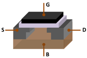
Dawon Kahng (Korean: 강대원; May 4, 1931 – May 13, 1992) was a Korean-American electrical engineer and inventor, known for his work in solid-state electronics. He is best known for inventing the MOSFET (metal–oxide–semiconductor field-effect transistor, or MOS transistor), along with his colleague Mohamed Atalla, in 1959. Kahng and Atalla developed both the PMOS and NMOS processes for MOSFET semiconductor device fabrication. The MOSFET is the most widely used type of transistor, and the basic element in most modern electronic equipment.
Kahng and Atalla later proposed the concept of the MOS integrated circuit, and they did pioneering work on Schottky diodes and nanolayer-base transistors in the early 1960s. Kahng then invented the floating-gate MOSFET (FGMOS) with Simon Min Sze in 1967. Kahng and Sze proposed that FGMOS could be used as floating-gate memory cells for non-volatile memory (NVM) and reprogrammable read-only memory (ROM), which became the basis for EPROM (erasable programmable ROM), EEPROM (electrically erasable programmable ROM) and flash memory technologies. Kahng was inducted into the National Inventors Hall of Fame in 2009.
Biography
Dawon Kahng was born on May 4, 1931, in Keijō, Keiki-dō, Korea, Empire of Japan (now Seoul, South Korea). He studied physics at Seoul National University in South Korea, and immigrated to the United States in 1955 to attend Ohio State University, where he received a doctorate in electrical engineering in 1959.
He was a researcher at Bell Telephone Laboratories in Murray Hill, New Jersey, and he invented MOSFET (metal–oxide–semiconductor field-effect transistor), which is the basic element in most of today's electronic equipment, with Mohamed Atalla in 1959. They fabricated both PMOS and NMOS devices with a 20 μm process.
Extending their work on MOS technology, Kahng and Atalla next did pioneering work on hot carrier devices, which used what would later be called a Schottky barrier. The Schottky diode, also known as the Schottky-barrier diode, was theorized for years, but was first practically realized as a result of the work of Kahng and Atalla during 1960–1961. They published their results in 1962 and called their device the "hot electron" triode structure with semiconductor-metal emitter. The Schottky diode went on to assume a prominent role in mixer applications. They later conducted further research on high-frequency Schottky diodes.
In 1962, Kahng and Atalla proposed and demonstrated an early metal nanolayer-base transistor. This device has a metallic layer with nanometric thickness sandwiched between two semiconducting layers, with the metal forming the base and the semiconductors forming the emitter and collector. With its low resistance and short transit times in the thin metallic nanolayer base, the device was capable of high operation frequency compared to bipolar transistors. Their pioneering work involved depositing metal layers (the base) on top of single crystal semiconductor substrates (the collector), with the emitter being a crystalline semiconductor piece with a top or a blunt corner pressed against the metallic layer (the point contact). They deposited gold (Au) thin films with a thickness of 10 nm on n-type germanium (n-Ge), while the point contact was n-type silicon (n-Si).
Along with his colleague Simon Min Sze, he invented the floating-gate MOSFET, which they first reported in 1967. They also invented the floating-gate memory cell, the foundation for many forms of semiconductor memory devices. He invented floating-gate non-volatile memory in 1967, and proposed that the floating gate of an MOS semiconductor device could be used for the cell of a reprogrammable ROM, which became the basis for EPROM (erasable programmable ROM), EEPROM (electrically erasable programmable ROM) and flash memory technologies. He also conducted research on ferro-electric semiconductors and luminous materials, and made important contributions to the field of electroluminescence.
After retiring from Bell Laboratories, he became the founding president of the NEC Research Institute in New Jersey. He was a fellow of the IEEE and a fellow of the Bell Laboratories. He was also a recipient of the Stuart Ballantine Medal of the Franklin Institute and the Distinguished Alumnus Award of the Ohio State University College of Engineering. He died of complications following emergency surgery for a ruptured aortic aneurysm in 1992.
Awards and honors
Kahng and Mohamed Atalla were awarded the Stuart Ballantine Medal at the 1975 Franklin Institute Awards, for their invention of the MOSFET. In 2009, Kahng was inducted into the National Inventors Hall of Fame. In 2014, the 1959 invention of the MOSFET was included on the list of IEEE milestones in electronics.


