MOSFET facts for kids
A MOSFET is an electronic component that acts as an electrically-controlled switch.
MOSFET stands for metal-oxide-semiconductor field-effect transistor. Transistors are small electrical devices that are used in, amongst other things, alarm clocks, calculators, and, perhaps most famously, computers; they are some of the most basic building blocks of modern electronics. A few MOSFETs amplify or process analog signals. Most are used in digital electronics.
MOSFETs act like valves for electricity. They have one input connection (the "gate") which is used to control the flow of electricity between two other connections (the "source" and "drain"). Said another way, the gate acts as a switch that controls the two outputs. Think of a dimmable light switch: the knob itself selects 'ON', 'OFF', or somewhere in between, controlling the brightness of the light. Think of a MOSFET in place of the light switch: the switch itself is the "gate", the "source" is the power coming into the house, and the "drain" is the light bulb.
The name MOSFET describes the structure and the function of the transistor. MOS refers to the fact that a MOSFET is built by layering metal (the "gate") on oxide (an insulator which prevents the flow of electricity) on semiconductor (the "source" and "drain"). FET describes the action of the gate on the semiconductor. An electric signal is sent to the gate, which creates an electric field that alters the connection between the "source" and "drain".
Almost all MOSFETs are used in integrated circuits. As of 2008, it is possible to fit 2,000,000,000 transistors on a single integrated circuit. In 1970, that number was around 2,000.
Contents
Operation
There are four common types of MOSFET:
Enhancement mode N-Channel MOSFET
The switch between the "source" and "drain" is usually off. You can turn the switch on by applying a positive voltage to the "gate", so it is higher voltage than the "source".
Enhancement mode P-Channel MOSFET
The switch between the "source" and "drain" is usually off. You can turn the switch on by applying a negative voltage to the "gate", so it is lower voltage than the "source".
Depletion mode N-Channel MOSFET
The switch between the "source" and "drain" is usually on. You can turn the switch off by applying a negative voltage to the "gate", so it is lower voltage than the "source".
Depletion mode P-Channel MOSFET
The switch between the "source" and "drain" is usually on. You can turn the switch off by applying a positive voltage to the "gate", so it is higher voltage than the "source".
Depletion mode P-Channel MOSFETs are not usually available.
Summary
| MOSFET Type | Normally | To change, apply ____ voltage to the "gate" |
|---|---|---|
| Enhancement mode N-Channel | Off | Positive |
| Enhancement mode P-Channel | Off | Negative |
| Depletion mode N-Channel | On | Negative |
| Depletion mode P-Channel | On | Positive |
Differences between MOSFETs
Integrated circuits
A small piece of silicon can have millions of MOSFETs created on it. This makes an integrated circuit. See the integrated circuit article for details.
The rest of this section is about single MOSFETs with three connections.
Heat
If the MOSFET is partly on, it will reduce the power going through it. It does that by converting some power into heat. Even if it is on, it will still convert some power to heat.
The MOSFET has a resistance. When current flows from the MOSFET's drain to it's source, there will be a voltage drop. Multiply that current and voltage to get the power loss. That lost power becomes heat.
The MOSFET must get rid of that heat, usually by passing it into the air.
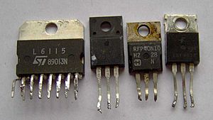
Smaller MOSFETs warm up and heat the nearby air. Some MOSFETs must be on a circuit board, which has a larger area to heat more air. The highest-power MOSFETs must be on a heatsink. The heatsink is a large piece of metal with fins to transfer the heat to the air over a large area. They may also need a fan to push lots of air over the heatsink.
Other differences between MOSFETs
There are lots of different MOSFETs available. When choosing a MOSFET, once you have decided among the 4 main types, there are lots of other things to think about. Differences between MOSFETs include:
- VGSS - The allowed voltage between the gate and source. If you apply too large a voltage, the MOSFET will break.
- VDSS - The allowed voltage between the drain and source. If you apply too large a voltage, the MOSFET will break.
- ID - The allowed current between the drain and source. If you are trying to power a large load, such as a motor, then you need a MOSFET designed for high currents.
- VGS(TH) ("Threshold voltage") - Approximately how big a voltage you need to apply to the "gate" for it to switch. How much the MOSFET is "on" depends on the exact voltage at the "gate", the temperature, and the voltage at the "drain". The datasheet for the MOSFET will have details.
- RDS(ON) - When the MOSFET is fully "on", it will act like a resistor with this value. A higher value means, when the MOSFET is fully "on", there is more wasted power and more heat. Smaller is better.
- PD - The largest amount of heat that the MOSFET can give off every second without breaking. (The "power dissipation"). If you make the MOSFET give off heat faster than this, then the MOSFET will overheat and break.
- RθJA - How bad the MOSFET is at transferring that heat to the air. Lower numbers are better. For MOSFETs that use a heatsink, they will say how bad they are at transferring heat to the heatsink.
- TJ - The working temperature of the part of the MOSFET that is generating the heat. If you make it go above the limit, the MOSFET will break.
- tD(ON) and tD(OFF) - The time it takes to turn the MOSFET on and off. Smaller, low voltage and low current MOSFETs, can be fast enough to use in the fastest computers. Larger, higher power MOSFETs, tend to be slower.
- Static electricity can break a MOSFET. Some MOSFETs include protection against static electricity.
- Some parts include several MOSFETs on a single device. This can be smaller than having separate MOSFETs. It can also be cheaper to make an electronic circuit board with less parts.
Theory
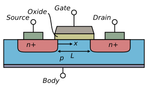
There are many different ways to make MOSFETs on the semiconductor. The simplest method is shown in the diagram to the right of this text. The blue part represents P-type silicon, while the red part represents N-type silicon. The intersection of the two types makes a diode. In silicon semiconductor, there is a quirk called the "Depletion Region". In doped silicon, with one part being doped N-Type, and one part being doped P-Type, a depletion region will naturally form on the intersection between the two. This is because of their acceptors and donors. P-type silicon has acceptors, also known as holes, which attract electrons towards them. The N-Type silicon has donors, or electrons, which are attracted to holes. In the border between the two, the electrons from the N-Type fill the holes in the P-type. This results in the acceptor, or P-type atoms becoming negatively charged, and since negative charges attract positive charges, acceptors, or holes, will flow towards the "junction". On the N-Type side, there is a positive charge, which results in the donors, or electrons, flowing towards the "junction." When they get there, they will be repelled by the negative charge on the other side of the junction, since alike charges repel. The same will happen on the P-Type side, the donors, or holes will be repelled by the positive area in the N type side. No electricity can flow between the two, since no electrons can move to the other side.
MOSFETs use this to their advantage. The "Body" of the MOSFET is powered negatively, which widens the depletion region, since the holes are filled with the new electrons, so the opposite force to the electrons on the N side becomes much larger. The "Source" of the MOSFET is powered negatively, which shrinks the depletion zone in the N type entirely, since there are enough electrons to fulfill the positive depletion zone. The "Drain" has a positive power. When the "Gate" is supplied with positive power, it will make a small electromagnetic field, which will remove the depletion zone directly below the gate, since there will be a "spray" of holes, which will make something called an "N-Channel". The N-Channel is a temporary region of the P-Type silicon area where there is no depletion zone. The positive electric field will neutralize all of the spare electrons that make up the depletion zone. The electrons in the source area will then have a clear way to move to the "Drain", which would make electricity flow from source to drain.
Images for kids
-
Channel formation in nMOS MOSFET shown as band diagram: Top panels: An applied gate voltage bends bands, depleting holes from surface (left). The charge inducing the bending is balanced by a layer of negative acceptor-ion charge (right). Bottom panel: A larger applied voltage further depletes holes but conduction band lowers enough in energy to populate a conducting channel
See also
 In Spanish: Transistor de efecto de campo metal-óxido-semiconductor para niños


