Paul Midgley facts for kids
Quick facts for kids
Paul Midgley
|
|
|---|---|

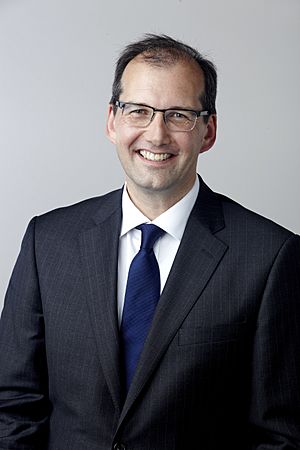
Paul Midgley in 2014, portrait via the Royal Society
|
|
| Born |
Paul Anthony Midgley
22 March 1966 |
| Alma mater | University of Bristol (BSc, MSc, PhD) |
| Awards |
|
| Scientific career | |
| Fields |
|
| Institutions | |
| Thesis | Electron microscopy of high Tc superconductors and related oxides (1991) |
Paul Anthony Midgley (born 1966) FRS is a Professor of Materials Science in the Department of Materials Science and Metallurgy at the University of Cambridge and a fellow of Peterhouse, Cambridge.
Contents
Education
Midgley was educated at the University of Bristol where he was awarded a Master of Science degree in 1988 and a PhD in 1991 for work on electron microscopy of high-temperature superconductors.
Career
Before moving to Cambridge in 1997, Midgley held two postdoctoral research fellowships in the Henry Herbert Wills Physics Laboratory at the University of Bristol.
Research
Midgley's research interests are in electron tomography, electron holography, energy-filtered imaging and ab initio structure determination by electron diffraction. During his research, Midgley has collaborated with Mark Welland, Rafal Dunin-Borkowski, Neil Mathur, John Meurig Thomas, Brian F. G. Johnson and Henning Sirringhaus.
Midgley's research has been funded by the Engineering and Physical Sciences Research Council (EPSRC), the Royal Commission for the Exhibition of 1851 and the Royal Society.
Awards and honours
Midgley was elected a Fellow of the Royal Society (FRS) in 2014. His nomination reads:
Midgley is distinguished for many innovations and impressive applications of transmission microscopy, diffraction and spectroscopy, particularly the pioneering development of sub-nanometre-scale electron tomography. His combination of high-angle dark field tomography and spectroscopy revolutionises the 3-d characterisation of materials and heterogeneous catalysts. He has successfully mapped dislocation networks with diffraction contrast tomography. With his world leading position in medium resolution electron holography, he has been able to combine this with tomography in 3-d mapping of electric fields and dopant distributions in semiconductor devices. His brilliant applications of electron diffraction to sub-micron structures, heavy fermion systems and mixed-valent manganites were important breakthroughs.

