
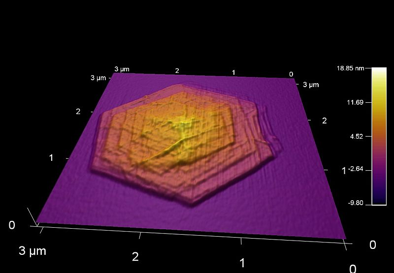
Image: Palladium nanosheet on silicon wafer

Size of this preview: 800 × 555 pixels. Other resolutions: 320 × 222 pixels | 1,231 × 854 pixels.
Original image (1,231 × 854 pixels, file size: 83 KB, MIME type: image/jpeg)
Description: 3D AFM tomography images of multilayered Palladium nanosheet on silicon wafer.
Title: Palladium nanosheet on silicon wafer
Credit: Own work[1]X. Yin, M. Shi, J. Wu, D. L. Gray, J. A. Bertke, H. Yang, “Quantitative analysis of different formation modes of platinum nanocrystals controlled by ligand chemistry”, Nano Letters, 2017, 17 (10), 6146–6150
Author: Xi Yin
Usage Terms: Creative Commons Attribution-Share Alike 4.0
License: CC BY-SA 4.0
License Link: https://creativecommons.org/licenses/by-sa/4.0
Attribution Required?: Yes
Image usage
The following page links to this image:

All content from Kiddle encyclopedia articles (including the article images and facts) can be freely used under Attribution-ShareAlike license, unless stated otherwise.