
Image: Bga und via IMGP4531 wp

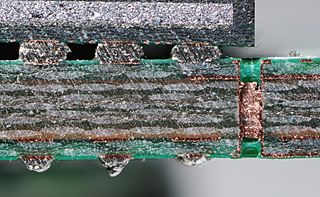
Size of this preview: 800 × 493 pixels. Other resolutions: 320 × 197 pixels | 2,000 × 1,232 pixels.
Original image (2,000 × 1,232 pixels, file size: 1.16 MB, MIME type: image/jpeg)
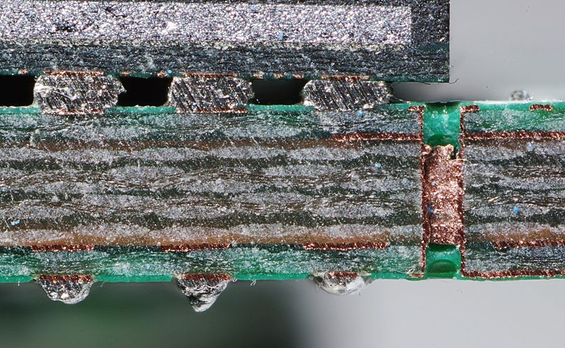
Description: Cut through an SDRAM-Module. It is a multi-layer Printed Circuit Board (PCB) with BGA-packaging. On the right side a via.
Title: Bga und via IMGP4531 wp
Credit: Own work
Author: Smial
Usage Terms: Free Art License
License: FAL
License Link: http://artlibre.org/licence/lal/en
Attribution Required?: Yes
Image usage
The following 2 pages link to this image:

All content from Kiddle encyclopedia articles (including the article images and facts) can be freely used under Attribution-ShareAlike license, unless stated otherwise.